Getting my VIA Expansion to Work with the Commodore 64
In my last post, I discussed wiring up a modern Versatile Interface Adapter to the expansion port of the Commodore 64. Unfortunately, I ran into timing issues and the design did not work. In this post, we’ll get it to work with the help of two extra chips, a breadboard, and a bunch of ribbon cable.

One idea for a fix is to take a page from the playbook of the Complex Interface adapter (CIA). As we saw in the last post, the CIA grabs the address values off the bus on the falling edge of its chip select signal. A possible solution would be to create a new clock signal for the VIA by funneling the regular clock (PHI2) and a negated chip select signal through an AND gate. That would effectively make the signals transition at the same time this new “clock” has its rising edge. There are two caveats with this solution. First, the VIA would not get an actual clock signal: the signal would only be active when the chip is selected, resulting in features such as timers or shift registers to no longer work. Next, in contrast to the CIA, the VIA requires a setup time of 8 nanoseconds, meaning the buses need to have the right value at least 8 nanoseconds before the rising edge of PHI2. To accomplish this, we could route the signal through a couple of gates or buffers to introduce a sufficient delay. Or a similar option would be to create a delayed PHI2 signal and combine it with an AND gate with the original PHI2 (assuming we can get the timing right).
Instead, I had another idea. There is another clock signal available on the expansion port, the dot clock. The dot clock is the pixel clock of the C64’s graphic chip, i.e. the frequency at which pixels are pushed to the screen. It’s about 8 MHz, 8 times the frequency of PHI2.
The idea is to clock a flip-flop with the dot clock and use it to store the value of PHI2. That results in a delayed PHI2 signal. Then, that signal is combined through an AND gate with the original PHI2 signal. The result is a clock with the same frequency as PHI2 but with a smaller duty cycle. Due to the smaller duty cycle (PHI2 is not at the high level for as long), there’s less time for the VIA. However, the VIA is rated for up to 14 MHz, so this won’t be a problem.
One complication: I already had a couple of shift registers on order (74AHCT595), so I am using one of those. This device can be wired up to act as two flip-flops in series. So instead of cutting one quarter of the duty cycle off, this setup will cut off one half.
The output of the shift register and the original PHI2 get routed through an AND gate. For this, I am using a 74AHC08 IC. The output from the shift register is already a signal with CMOS logic levels and for PHI2 I am using the output from the 74HCT244 buffer (see last post). Since there are no signals with TTL logic levels, an AHC instead of an AHCT device will do (it is faster, too).

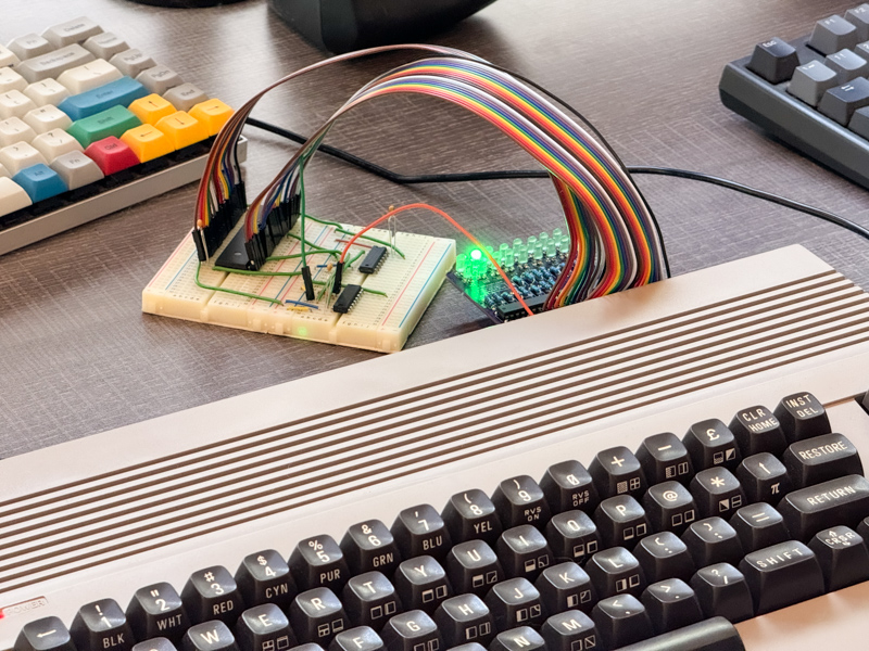
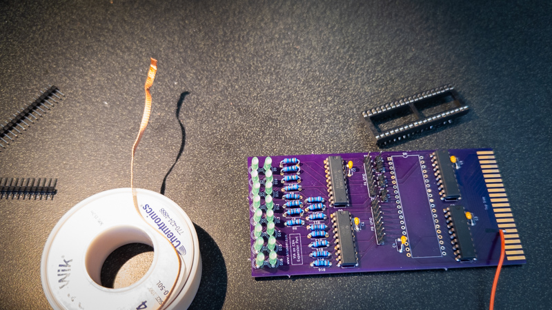
To implement this idea, I had to first remove the VIA from its socket on the PCB and then unsolder the socket. In addition, I soldered a wire to the dot clock signal on the PCB edge connector. Instead of the socket, I soldered in two 20-pin headers. With that I could bring all signals of the VIA to a breadboard using a bunch of jumper wires. On the breadboard, the VIA is connected to all the signals exactly as on the PCB with the exception of PHI2, which now gets funneled through the shift register and the AND gate.

Before plugging the VIA into the breadboard, I took a look at the signals with my logic analyzer (see screenshot above). NPHI2 is the modified PHI2 signal. In contrast to before, the CS2B signal (and similarly the address lines) have now the correct value during the full duration of NPHI2 being high. At the bottom you can see the 8 MHz dot clock signal.

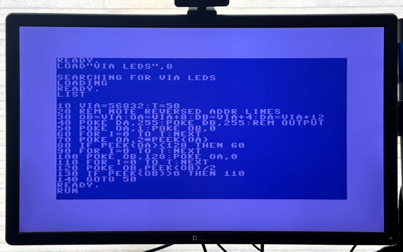
Then it was time to plug the VIA into the breadboard. Some quick checks on the C64 confirmed that now everything worked as expected. I was able to write values into the VIA registers and read them back. And setting the ORA and ORB registers allowed turning on the LEDs as expected. To make it visually more interesting, I wrote a BASIC program to have a light run in a circle counterclockwise. You can see the result in the video below.
And this concludes this little exercise. It’s not a single PCB anymore since there’s now a breadboard dangling off it, but the VIA does its job. If you have suggestions or corrections, please hit me up on Mastodon.
Subscribe via RSS